

Manufacturer

THE PREFERRED
bUSINESS PARTNER
THE PREFERRED
bUSINESS PARTNER
NEWS
The centrality of your PCB
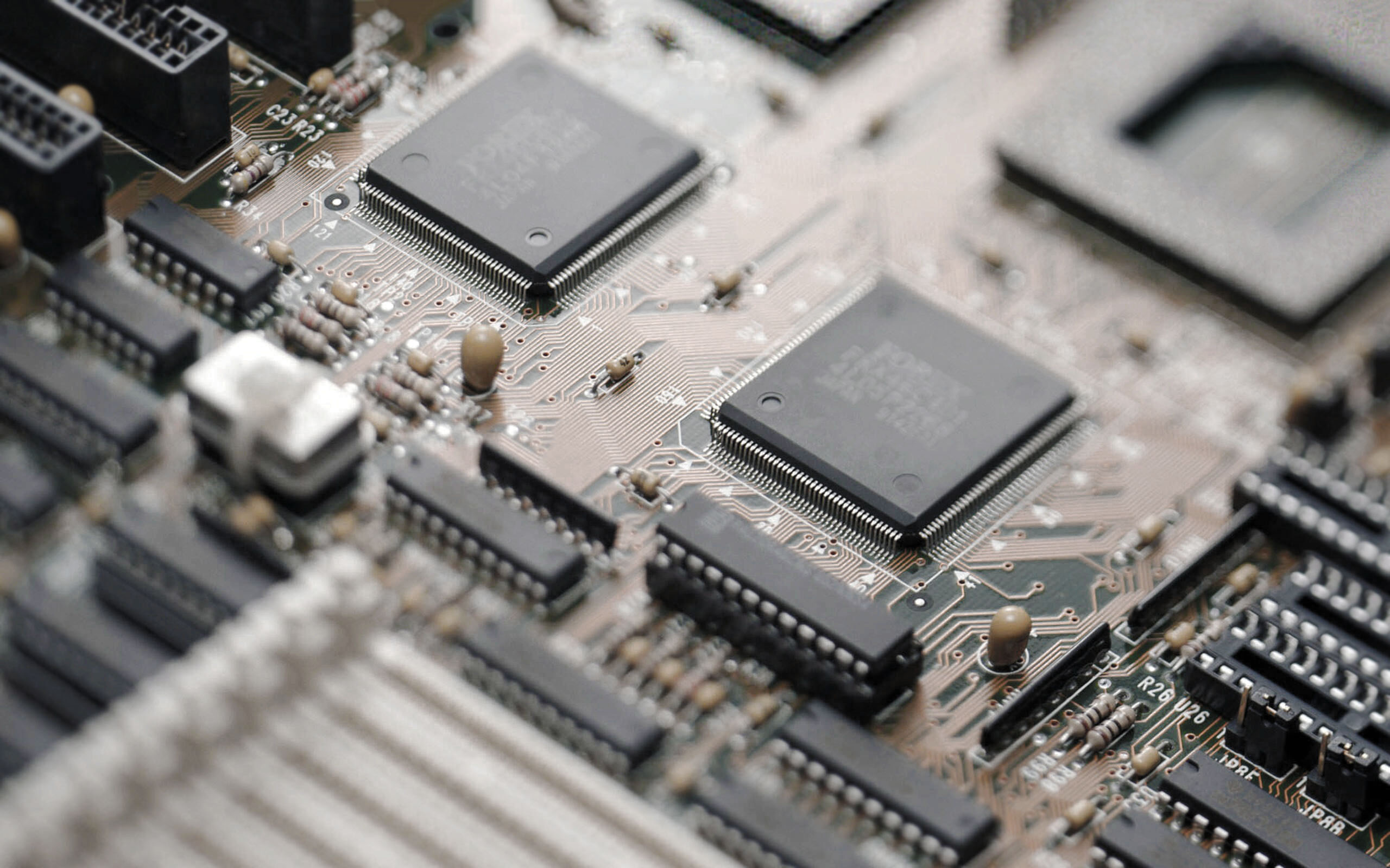
My mentor, Big John Massa, taught me the centrality of the PCB to a design effort. Massa was always looking for new ways to design and build circuit boards. When our peers were talking about instruction-caching architectures in 68020 chips, Massa was talking about circuit board layout programs and overnight prototyping.
Massa noted, “In my 40 years doing electronics, it’s always the circuit board that is the holdup and the limiting factor of every project.” You don’t just make a pile of schematics for a living. You have a higher obligation to see that those schematics turn into something that can be built and sold.
The modern PCB is not just a schedule killer, it’s a critical component that has precise design requirements. The operating frequencies and rise- and fall-times of the signals in electronics are faster and faster. So the PCB has become more and more important.
CONTACT US
ABOUT ANYTHING RELATED TO OUR PRODUCTS OR SERVICES.
WE'LL DO OUR BEST GET BACK TO YOU AS SOON AS POSSIBLE.
unit c, 9/f winning house, NO. 72-76 SUZHOU TECHNOGREEN ELECTRONIC CO., LTD.
WING LOK STREET, SHEUNG WAN, hk. No.1702, BlocK 1, XINGHAI BUSINESS SQUARE,
Tel: +852 3110 3290 SUZHOU INDUSTRIAL PARK, CHINA.
HP : +86 182 6166 8027 TEL/FAX : +86 512 6507 1482
FAX: +852 3110 3291 HP : +86 182 6166 8027
EMAIL:info@ally-circuit.com email : marketing@technogreen.cn

Copyright © 2009-2011, www.ALLY-CIRCUIT.com, All rights reserved


