


Manufacturer

THE PREFERRED
bUSINESS PARTNER
THE PREFERRED
bUSINESS PARTNER
NEWS
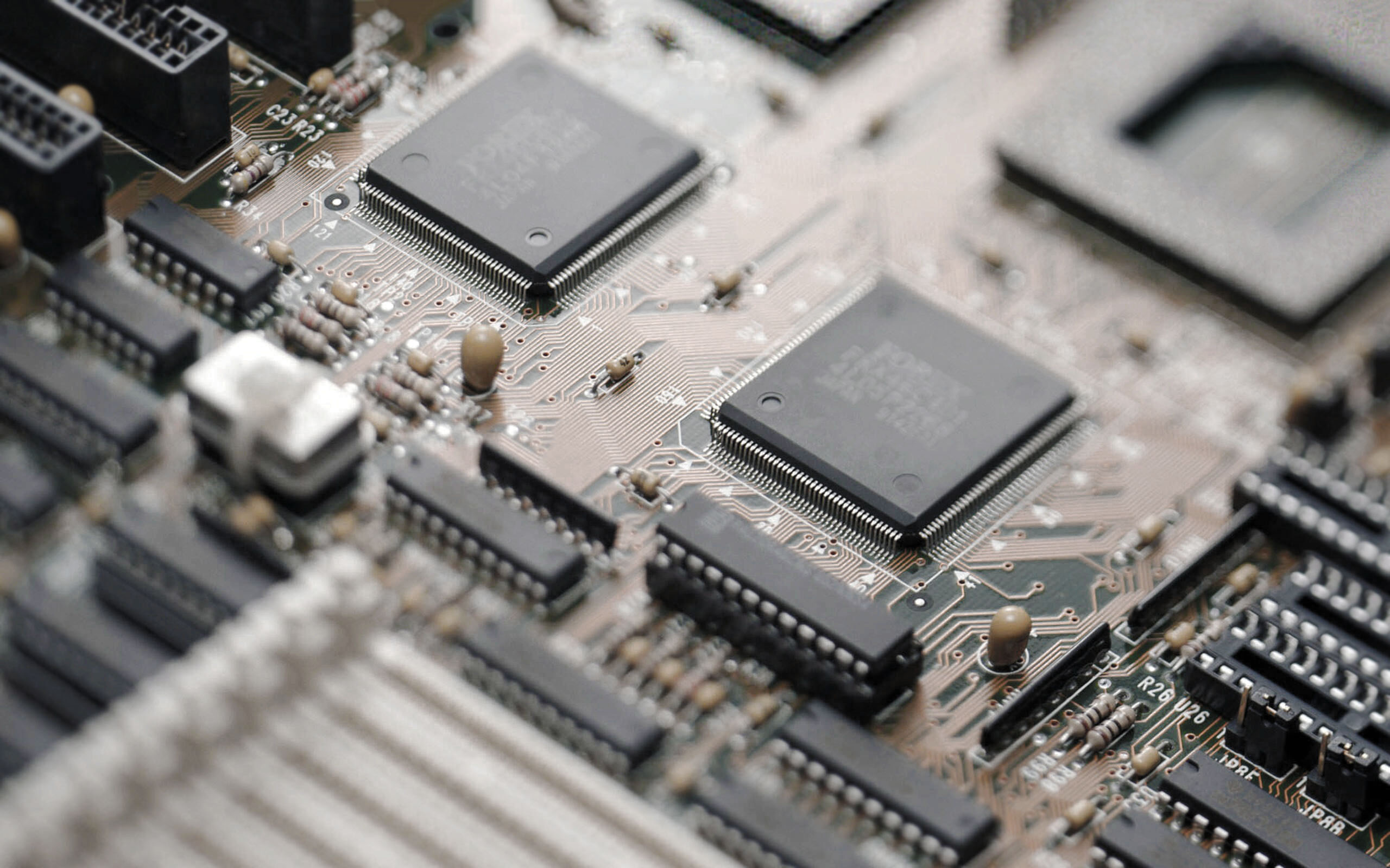
When it comes to developing the pieces of hardware, the process is not so simple. And, when it comes to printed circuit board (PCB) development efforts, the process becomes even more challenging. That's because PCBs are the launching points for hardware product development and the laminate and prepreg materials used in designing and manufacturing PCBs are the nuclei for those boards. (Prepreg is fiberglass cloth that has been saturated with resin that is not fully cured. As a PCB is placed under the heat and pressure of lamination this resin melts and flows into the voids in the adjacent copper layers filling them.)

The global aspects of the PCB development process are pretty much carved in stone—design and prototype the product in the U.S. and then move volume production offshore. The challenge lies in ensuring that the laminates and prepregs used for US prototyping efforts will be the same as those used in offshore volume production. On the surface, the seamless transparent transition process for utilizing the same PCB laminates from prototype to the full up product processes should be a "no brainer" and one that should not be subject to much scrutiny but that is not the case. This article will discuss what takes place in today's design/prototyping environments and the challenges that ensue in the realm of volume production.
What's different?
When electronic products were not nearly as complex as they are now laminate and prepreg selection was not that big of a deal. Almost everything could be done using some iteration of FR-4 class material. Products were forgiving enough that using an FR-4 class material for the U.S. prototyping effort and then moving to a similar but not identical iteration of it for off-shore volume production was o.k. Specifically, it was, and often still is, the practice of off-shore volume manufacturers to substitute the materials that are called out on the stackup drawings provided as guidelines for PCB fabrication. In fact, in some instances, product development companies have welcomed the opportunity to save money wherever or however they can and having offshore fabricators switch to a lower-cost, similar but not necessarily totally equivalent material is one path to realizing these savings. So, let's forward to today's product development environments. High-speed boards once occupied the niche of select, sophisticated pieces of hardware. But, by virtue of the components mounted onto it, today, every PCB is high-speed regardless of its final product implementation. And, as has been pointed out in a number of articles, technical presentations and conference panels, in many instances, we are bumping up against what is achievable in terms of performance parameters in even the fastest of the high speed laminates. There is not much more "there, there" in moving up the performance curve with laminate materials. The next step is photo optics but this is a huge step requiring massive changes in not just design processes but also in equipment tooling and manufacturing operations. Simply put, the transition to photo optics is not technically or economically feasible at this point in time. As a result, we are often called upon to wring the last ounce of performance capabilities out of existing laminate materials. As a consulting firm, Speeding Edge is frequently exhorted to try and exercise some Rocky/Bullwinkle "watch me pull a rabbit out of my hat" magic that really pushes the envelope in terms of what is practicable.

One of the factors that come into play is an unrealistic attempt to place burdens upon board fabricators. Rather than specifying certain materials, some product developers call upon board fabricators to achieve a certain performance curve. This is not and never can be the role of board manufacturers. In addition, in the process of specifying certain performance matrices over a particular laminate designation crucial factors such as glass-weave induced skew have, at best , been overlooked and, at worst, totally ignored.
Because PCBs are often viewed as commodity items that don't require careful design and manufacture, the tendency has been for product developers to go the route of what's the fastest and cheapest way to go either in the bare board manufacturing processes or in the board-to-chip connections. Several years back in the global supply chain world of component manufacturing, FPGA suppliers opted to use third-party chip carriers in an attempt to keep costs down. The results were cataclysmic.
Because little attention was paid to the quality of these chip
carriers, the board- to-chip connections were unreliable. And, the
problems associated with these faulty connections weren't readily
traceable. The problems only occurred under certain operating conditions
and it took a fair amount of research (high non-recurring engineering
costs) to locate the source of the problems. What was even more dire is
that there was no fix to the problems because they occurred at the
interconnect level and there was no work around. Designs had to be
scrapped and started from scratch. Some companies missed critical market
windows. A few went out of business altogether. This was one time when,
as a consulting company, we found ourselves wishing that the phone
wasn't ringing off the hook because the answers to the questions were
not going to be good.
Who owns the problems?
Ownership is at the heart of the challenge in designing and manufacturing PCBs. Electronic product companies have huge software development teams and small or non-existent hardware development teams (this is what keeps engineering consultants in business). Little or no emphasis is put upon the laminate and prepreg selection process so product engineers aren't always sure which laminate properties are the most important for their particular designs. Or as noted above, in an even growing number of cases, they are designing products that are really pushing the parameters of laminate properties and what can be achieved within their confines. They don't want the answer to be that their products, as they are designed, are not readily manufacturable using widely available, current technology.

Laminate suppliers also share responsibility. They need to provide all of the relevant information necessary to ensure that product development engineers are making the right selection for their particular product implementation and that there are sufficient quantities of materials available within the global supply chain to meet those requirements. On their websites, laminate suppliers need to provide in very clear, easy-to-access information all of the information a product developer needs to have such as technical data sheets, processing guidelines, laminate and prepreg lineups with glass weave styles, resin content, dielectric constant and loss tangent to select the best material for his/her design.
And, fabricators need to be able to show that they have the processes in place to manufacture boards using certain laminates. This is no simple task. Laminates and prepregs need to be qualified to a fabricator's processes and capabilities. There are a number of qualification hoops which a PCB fabricator needs to jump through and, in a global supply chain world, the fabricator needs to know that there will be enough product demand to warrant going through these hoops.
So, the end goal for PCB production is fairly straight forward--ensure that the laminates used in U.S. protoptyping efforts will remain the same for off-shore volume production. But there are issues and challenges associated with achieving this goal in the global supply chain and they are similar to what they are for any aspect of product design. There are multiple layers to the problem; there are no easy answers or quick fixes and there are no miracle next-generation materials on the horizon that will satisfactorily address all of the issues. What is a given is the ownership of the issues and challenges stretches across the entire global supply chain world as well as the entire product development process. Communication in all forms—from product development groups to laminate suppliers to fabricators is the first, most critical step in the right direction of a journey that spans thousands of miles.
CONTACT US
ABOUT ANYTHING RELATED TO OUR PRODUCTS OR SERVICES.
WE'LL DO OUR BEST GET BACK TO YOU AS SOON AS POSSIBLE.
unit c, 9/f winning house, NO. 72-76 SUZHOU TECHNOGREEN ELECTRONIC CO., LTD.
WING LOK STREET, SHEUNG WAN, hk. No.1702, BlocK 1, XINGHAI BUSINESS SQUARE,
Tel: +852 3110 3290 SUZHOU INDUSTRIAL PARK, CHINA.
HP : +86 182 6166 8027 TEL/FAX : +86 512 6507 1482
FAX: +852 3110 3291 HP : +86 182 6166 8027
EMAIL:info@ally-circuit.com email : marketing@technogreen.cn

Copyright © 2009-2011, www.ALLY-CIRCUIT.com, All rights reserved